Search PXDRIVE
wrt150n board and chips numbered - picture uploaded by yazeed to people
pxdrive.com -> yazeed -> wrt150n board and chips numbered
| wrt150n board and chips numbered | |||||||||||||||
| So by the numbers, the chips are
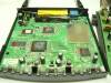
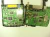
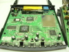
1- This chip has a sticker that reads VER:1.01.9 CS: 7A9F Under the sticker Spansion S29AL032D90TF103 0719EBM G © spansion 2- Hynix 715U C HY5DU281622FTP-5 KOR HCER1257HQ5 3-BROADCOM BCM4704KPBG CK0713 P12 817031 R2 4-BROADCOM BCM5325FKQMG RG0646 P11 802936 1A 5-BRAODCOM BCM4321LKFBG UN0722 P21 824300 N3 A final chip is hidden under the sheild, it is a BROADCOM BCM2055KFB6 (COULD BE BCM2055KF86) HE0719 P20 822522 N3 i could not find much info about this chip so good luck And therefore, chip #1 is "4MB Flash RAM chip.", Chip #2 is a SSTL_2 interface compatible 16MB DD RAM chip ! wow did i just say that !, Chip #3 is the CPU of the system, Chip #4 is the 10/100 switch processor, And chip #5 is the WLAN DSP processor ! Those are all the chips i can see that are worth mentioning from a software point of view | |||||||||||||||
| Voted 3.92/5 with 10 Votes | |||||||||||||||
| |||||||||||||||
| Picture URL: Medium URL: Thumbnail URL: | |||||||||||||||
| User Comments | |
| *ketan | 2009-03-08 21:24:03 - 48292 |
| what about other chips. | |
| I need to know about the 8 pin soic power chip used (buck boost converter)for the one on the right.It has 3 coils but 4 chips i want the one that is different.More details will help.*MASKED@EMAIL.ADRS* | |
Albums by first letter
A : B : C : D : E : F : G : H : I : J : K : L : M : N : O : P : Q : R : S : T : U : V : W : X : Y : Z : numbers : other
A : B : C : D : E : F : G : H : I : J : K : L : M : N : O : P : Q : R : S : T : U : V : W : X : Y : Z : numbers : other
My Drive
Private Images:
0 Bytes / 0 Bytes.

Public Images:
0 Bytes / 0 Bytes.
Steps:
- Register
- Once you enter your email address, You will get an Email, in that email you will find a link., Simply click the link, and chose a username and password
- You are now registered at the website and ready to upload and organise your photos and images
- Go to the upload page, and start uploading your pictures and photos
Popular albums
Private Domain Registration
Domain Name Reseller
Quality Domains
Star Academy 2011
Whois and Web Statistics
Domain Generator
LU Money
Domain Name Reseller
Quality Domains
Star Academy 2011
Whois and Web Statistics
Domain Generator
LU Money